IIoT for Semiconductor Manufacturing: How to Monitor Lithography, Etching, and Deposition Equipment in Real Time
A single hour of unplanned downtime in a semiconductor fab costs between $100,000 and $500,000. With equipment valued at $10–$50 million per tool and process tolerances measured in nanometers, semiconductor manufacturing demands the most precise equipment monitoring in any industry. IIoT platforms are transforming how fabs manage equipment health, predict failures, and protect yield — but the semiconductor environment has unique challenges that general-purpose monitoring tools weren't designed to handle.
Why Semiconductor Manufacturing Needs IIoT
Semiconductor fabrication is arguably the most complex manufacturing process on Earth. A modern chip goes through 400–700 process steps over 2–3 months, moving through lithography, etching, deposition, implantation, CMP (chemical-mechanical polishing), cleaning, and inspection — each requiring precise environmental control and equipment performance.
The stakes are enormous:
- Equipment utilization targets: Fabs target 85–95% uptime. Every percentage point of downtime costs millions annually.
- Yield sensitivity: A 1% yield improvement in a high-volume fab can be worth $10–$50 million per year.
- Process drift: Equipment that drifts even slightly out of specification produces defective wafers that aren't detected until inspection — days or weeks later.
- Recipe management: Modern fabs run hundreds of recipes across dozens of tools. Equipment behavior varies by recipe, making monitoring complex.
Critical Equipment to Monitor
Lithography Systems
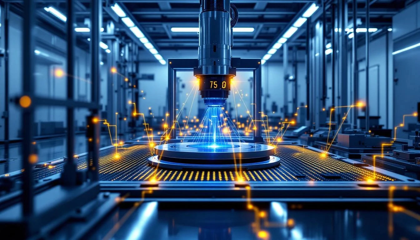
Lithography tools (EUV, DUV steppers and scanners) are the most expensive equipment in the fab — $150M+ for a single EUV system from ASML. Key monitoring parameters include:
- Laser source performance: Pulse energy stability, repetition rate, beam profile
- Lens contamination: Transmission degradation over time indicates lens cleaning or replacement needs
- Overlay accuracy: Alignment precision between layers directly impacts yield
- Environmental control: Temperature stability within ±0.01°C, humidity, and vibration isolation
- Reticle handling: Stage position accuracy, reticle flatness, contamination detection
IIoT monitoring of lithography systems focuses on tracking performance degradation trends. When laser pulse energy begins drifting or overlay measurements show systematic shifts, AI-powered analytics can predict when maintenance is needed — allowing fabs to schedule service during planned downtime windows rather than experiencing unexpected failures.
Etch Equipment
Plasma etch tools (RIE, ICP, capacitively-coupled) require monitoring of:
- Plasma uniformity: Non-uniform plasma produces non-uniform etch rates across the wafer
- Chamber pressure stability: Pressure excursions indicate gas delivery issues, pump degradation, or chamber leaks
- RF power delivery: Forward power, reflected power, and impedance matching network position
- Gas flow rates: MFC (mass flow controller) accuracy and response time
- Endpoint detection: Optical emission spectroscopy (OES) signals for etch endpoint accuracy
- Chamber seasoning: Etch rate drift after chamber cleans indicates conditioning status
CVD and PVD Systems
Chemical Vapor Deposition (CVD) and Physical Vapor Deposition (PVD) tools deposit thin films with nanometer-level thickness control:
- Deposition rate uniformity: Thickness variation across the wafer indicates source or gas distribution issues
- Source lifetime: Sputter targets, precursor levels, and showerhead condition degrade over time
- Vacuum integrity: Base pressure trends indicate outgassing, leaks, or pump degradation
- Temperature uniformity: Susceptor temperature uniformity directly affects film properties
- Particle levels: In-situ particle monitoring catches contamination before it reaches wafers
CMP Equipment
Chemical-Mechanical Polishing tools require real-time monitoring of:
- Pad conditioning: Diamond conditioner wear affects polishing rate and uniformity
- Slurry delivery: Flow rate, concentration, and temperature of polishing slurry
- Down force and back pressure: Polishing pressure profiles across the wafer
- Motor current signatures: Changes in platen or carrier motor current indicate pad wear or process drift
- Endpoint detection: In-situ thickness monitoring for automatic polish stop
Clean Room Environmental Systems
The fab environment itself requires continuous monitoring:
- Particle counts: Class 1/ISO 3 clean rooms require real-time particle monitoring at multiple points
- Temperature and humidity: Tight control (typically 21±0.5°C, 45±5% RH) across the entire fab
- Vibration levels: Nanometer-scale lithography requires vibration isolation monitoring
- Air flow: Laminar flow velocity and uniformity in process bays
- Chemical air monitoring: VOC and hazardous gas detection for safety and process integrity
IIoT Architecture for Semiconductor Fabs
Semiconductor fabs have unique IT/OT requirements that affect IIoT deployment:
Data Volume and Velocity
A single semiconductor tool can generate 1–10 GB of data per day. A 300mm fab with 500 tools produces terabytes daily. IIoT platforms must handle this data velocity without introducing latency that could delay fault detection.
SEMI Standards Compliance
The semiconductor industry has specific equipment communication standards:
- SECS/GEM (SEMI E5/E30): Equipment communication standard for host-to-equipment messaging
- EDA/Interface A (SEMI E120-E164): High-speed equipment data acquisition for advanced analytics
- GEM300 (SEMI E40/E87/E90/E94/E116): 300mm fab automation standards
Any IIoT platform targeting semiconductor must support or integrate with these standards. General-purpose platforms that only support OPC UA or Modbus miss the semiconductor-specific data that matters most.
Fault Detection and Classification (FDC)
FDC is the semiconductor industry's term for real-time equipment monitoring. Key capabilities include:
- Univariate monitoring: Tracking individual parameters against control limits (SPC charts)
- Multivariate monitoring: Detecting complex fault signatures that span multiple parameters simultaneously
- Trace-level analysis: Monitoring parameter behavior within each processing step, not just summary statistics
- Golden trace comparison: Comparing current processing traces against known-good reference traces
- Virtual metrology: Predicting wafer measurements from equipment data, reducing physical inspection
Predictive Maintenance in Semiconductor Fabs
Predictive maintenance in semiconductor manufacturing goes beyond simple condition monitoring. The challenges include:
PM Scheduling Optimization
Semiconductor equipment requires periodic preventive maintenance (chamber cleans, source changes, calibrations). The question is when:
- Too early: Wastes productive time and consumables
- Too late: Risks wafer defects or unplanned downtime
- Optimized: AI models predict the optimal PM timing based on actual equipment condition rather than fixed intervals
A well-implemented predictive maintenance program can extend mean time between PMs by 15–25%, directly increasing equipment availability.
Consumable Life Management
Semiconductor tools consume expensive parts: sputter targets, etch chamber liners, polishing pads, seals, filters. IIoT monitoring tracks consumable degradation rates and predicts replacement timing:
- Sputter targets: Track thickness remaining based on accumulated power-hours and deposition rate trends
- Etch chamber liners: Monitor etch rate drift that indicates liner degradation
- CMP pads: Track pad thickness, polishing rate, and conditioning groove depth
- Vacuum pumps: Monitor vibration, temperature, and current draw for pump health
Run-to-Run Control
IIoT data feeds into run-to-run (R2R) control systems that automatically adjust process recipes based on equipment condition and upstream wafer state. This closed-loop approach maintains process consistency even as equipment drifts between PMs.
ROI of IIoT in Semiconductor Manufacturing
The ROI of IIoT in semiconductor fabs is typically measured in three areas:
1. Unplanned Downtime Reduction
Reducing unplanned downtime by just 1% in a high-volume fab translates to:
- Additional wafer output: 500–2,000 additional wafer starts per year
- Revenue impact: $5–$50 million depending on product mix
- Typical IIoT impact: 15–30% reduction in unplanned downtime events
2. Yield Improvement
Catching equipment drift before it impacts wafers:
- Defect reduction: Early detection of particle excursions, process drift, and equipment faults
- Typical impact: 0.1–0.5% yield improvement from better FDC/APC
- Revenue impact: $2–$25 million annually in a high-volume fab
3. PM Optimization
Extending mean time between PMs while reducing PM-related wafer scrap:
- Additional productive hours: 200–500 hours per tool per year
- Reduced consumable waste: 10–20% savings on consumables
- Reduced qualification wafers: Fewer PM-triggered qual lots
Choosing an IIoT Platform for Semiconductor
The semiconductor industry's unique requirements limit the field of viable IIoT platforms. Key selection criteria:
- SECS/GEM and EDA integration — Can it consume semiconductor-specific equipment data?
- Data volume handling — Can it process terabytes of daily equipment data without lag?
- Trace-level analytics — Does it support within-recipe parameter monitoring?
- FDC capabilities — Built-in multivariate fault detection and classification?
- Integration with existing MES — Does it work alongside your fab execution system?
- Scalability — Can it scale from a pilot on 10 tools to fab-wide deployment on 500+?
MachineCDN for Semiconductor
MachineCDN's protocol-native approach connects directly to semiconductor equipment controllers, pulling real-time data without requiring additional middleware or integration layers. Key advantages for semiconductor:
- Direct PLC/controller connectivity — Native industrial protocols connect to equipment controllers
- AI-powered predictive maintenance — Machine learning models detect degradation patterns specific to your equipment
- 3-minute device setup — Edge devices connect without burdening fab IT
- Cellular connectivity — Bypasses the secure fab network entirely
- Fleet management — Monitor tools across multiple fab locations in a single dashboard
- Threshold alerting — Configurable approaching and active alerts with automatic escalation
The Bottom Line
Semiconductor manufacturing is the ultimate stress test for IIoT platforms. The data volumes are massive, the precision requirements are extreme, and the cost of equipment failures is measured in millions. But the ROI is equally compelling — even modest improvements in uptime and yield translate into enormous financial returns.
The key is choosing a platform that handles semiconductor's unique requirements while deploying fast enough to deliver value before the next technology node makes your current tooling obsolete.
Ready to bring IIoT intelligence to your fab? Book a demo and see how MachineCDN monitors manufacturing equipment in real time.